|
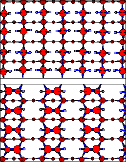
Fig.1A Bulk Terminated and
Reconstructed Si (001)-2 × 1 Surface. An
individual silicon atom can form four bonds with
neighboring atoms. In the bulk of a silicon crystal,
viewed from the (001) plane, two of these bonds reach to
the level below and two reach to the next level above.
The top figure shows three successive planes in the bulk
crystal structure (dots of different shades of red
represent atoms on different levels.) Cleaving a crystal
along a (001) plane leaves the surface atoms with only
two bonds intact and the other two dangling. The surface
atoms then swing toward neighboring atoms to form pairs,
known as dimers. The bottom figure shows the same Si
(001) plane reconstructed to form rows of dimers along
the surface. This leaves the reconstructed surface with
only two dangling bonds per dimer. At low temperatures
the dimer rows buckle so that alternating atoms are
slightly raised and lowered from the plane (this is shown
in the varying of dot sizes.) |

