In addition to studying the free terrace diffusion of Si dimers on the Si(001) surface, we used the tracking technique to investigate dimer dissociation and the interaction of a Si dimer with an A-type step-edge. Applying the tracking technique to studies of Si dimers on the Si(001)-2 × 1 surface has enabled us to resolve individual diffusive events. Studying these events has allowed us to set the activation energies for diffusion of a dimer along a substrate dimer row and trough, and place a lower bound of 1.40 eV on the activation energy for dimer dissociation. We have also observed the free energy of a dimer to decrease by 32 ± 2 meV at a site adjacent to an A-type step-edge.
![]()

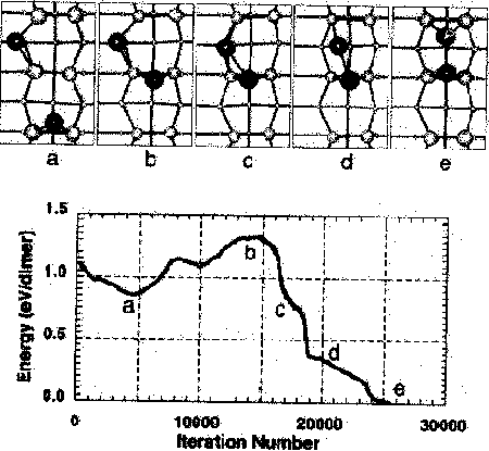
Fig. 1. The dissociation pathway considered by Yamasaki et al.While this depicts dimer formation, the same pathway could be followed in reverse for dimer dissociation. (Reproduced from Yamasaki et al.)
The population of dimers on the silicon surface depends on the activation energy for dimer dissociation. It is therefore important to determine the dissociation energy in order to evaluate dimers' importance in processes under different surface conditions. The theoretical calculations of Yamasaki et al. and Brocks et al. have addressed dissociation. Considering the pathway shown in Fig. 1, Yamasaki et al. have applied Car-Parinello modeling to estimate an activation energy of 1.33 eV.
Experimentally, we can set a lower bound on the dimer dissociation energy by observing a dimer which does not dissociate in time t. The observation time can be related to an energy bound by applying the Arrhenius relation,
Here R is the rate of dissociation, E is the associated activation energy, and v=1013Hz is the assumed attempt frequency. Not seeing a dissociation for time t implies that R<1/t, or
From conventional STM movies at 500 K for 4860 s we found a relatively height bound for E. However, conventional scanning requires that the tip spend only a small fraction of its scan-time over the dimer, so there is the possibility of a dimer's dissociation and reformation going undetected. Nearly continuous observation of a dimer is necessary to minimize this possibility. This is a good application for the tracking technique. By tracking a dimer at 423 K for 8640 s, we find E>1.40eV with a 95% confidence.
![]()
Central to any epitaxial growth model is an understanding of how the adsorbate in question interacts with islands, steps, and other surface features. As can be observed in conventional STM movies, it is not sufficient to assume that an adsorbate sticks with unit probability when it meets an atomic-height step; one must consider these interactions in more detail.
 |
Fig. 2. Schematic of the 1D potential for dimer motion along a substrate dimer row that terminates on the right at a type-A step.
We have observed dimers trapped between and on
top of surface islands (of single atomic height). We have also
observed that dimers spend a longer period of time in sites at
the bottom of step edges. These observations indicate the
existence of edge-site barriers and wells, as are depicted in
Fig. 2. The hop rates across the potential barriers in Fig. 2 are
related to those barriers by the Arrhenius relation: ED=KTln[vD/RD]
and ES=KT ln[vS/(2 RS)],
or ES - ED
= kT ln [RDvs/(2RSv
![]()
By applying the tracking technique to studies of Si dimer diffusion on the Si(001)-2 × 1 surface, we have resolved individual diffusive events. Studying these events has allowed us to set the activation energy for diffusion of a dimer along a substrate dimer row and trough, and place a lower bound of 1.40 eV on the activation energy for dimer dissociation. We have also observed the free energy of a dimer to decrease by 32 ± 2 meV at a site adjacent to a type-A edge. The tracking technique may be applied to the study of number of surface features and adsorbates on a variety of surfaces. As with our application to Si dimers a Si surface, the tracking technique promises to provide time resolutions of single feature processes that are unattainable by current conventional STM techniques.
![]()
G. Brocks, P. J. Kelly, and R. Car. Phys. Rev. Lett. 66, 1729 (1991.)
B.S. Swartzentruber, Phys. Rev. Lett. 76, 459 (1996.)
T. Yamasaki and T. Uda. Phys. Rev. Lett. 76, 2949-2952 (1996.)
* T. Uda. Presented at Japan-U.S. Seminar on Surface Dynamics and Structures in Epitaxial Growth. March 26, 1997.
![]()
This research was supported by National Science Foundation
Grant DMR 9222493.
Jump to
Across Rows Diffusion
Diffusion Along Rows
and Troughs
The Atom Tracking Technique
Hot STM Labs
Copyright 1997 by the Regents of the University of Minnesota