Selective nanoscale growth of titanium on the Si(001) surface using an atomic hydrogen resist
Nanoscale titanium structures are fabricated on a patterned Si(001)-(2×1) surface using an atomic hydrogen resist. The patterning is achieved by removing small areas of hydrogen with a scanning tunneling microscope. The large chemical reactivity of the bare Si surface compared to the hydrogen passivated surface provides selective area growth of titanium clusters grown by chemical vapor deposition using TiCl4. Titanium growth by chemical vapor deposition is normally limited by chlorine passivation of the bare Si surface. However, by removing the chlorine with the scanning tunneling microscope, the growth can be resumed.
_______________________________________
In recent years, scanning probe microscopes have been employed in nanolithography.(1) Among various scanning probe microscope nanolithography techniques, scanning tunneling microscope (STM) lithography has attracted attention because of its ability to make nanoscale surface modifications in an atomic resist layer. On the Si(001)-(2x1) surface, hydrogen and oxygen have both been used for resist layers. In the case of hydrogen, the Si surface is terminated by an atomic monohydride layer.(2,3) For oxygen, an ultra thin SiO2 film is formed.(4) The ultimate goal of the STM lithography is to complete a nanoscale toolkit for the fabrication of nanoscale structures and devices such as single electron transistors.
In 1994, Lyding et al. demonstrated the desorption of hydrogen from the Si(001)-(2×1) monohydride surface with the current from an STM tip. The high density and localization of the STM current make it possible to create a pattern on the nanometer scale by removing individual hydrogen atoms.(2) Recently, Dai et al utilized a carbon nanotube as a tip on an atomic force microscope to improve the reliability and increase the maximum lithographic writing speed to 0.5 mm/s.(5)
Pattern transfer has been demonstrated with aluminum (6) and gallium (7) evaporation, and also by selective chemical vapor deposition (CVD) of Fe,(8) Au,(3) Al,(3, 9) and norbornadiene.(3) Shen et al. reported that the difference in diffusion length of aluminum evaporated on bare and hydrogen terminated Si(001) leads to a seven to one enhancement in growth on bare Si(001). The difference in chemical reactivity of an aluminum precursor on these surfaces further improves the selectivity; an enhancement of at least 250 to 1 is observed for aluminum deposited by CVD.(9)
Titanium is used in a self-aligned silicide process to form titanium silicide (TiSi2) contacts on Si.(9) Titanium silicide has attracted attention as a source drain contact material because of its low contact and bulk resistivity and high thermal stability.(11) Controlling the silicide is a step towards the future technology of ultralarge-scale integration and nanoscale devices. In addition, there is interest in TiN as a diffusion barrier material between silicon/aluminum or silicon/copper interfaces because of its high conductivity and high thermal stability.(12) Furthermore, TiN serves as an effective nucleation layer for uniform growth of Al CVD on Si(001).(13) To produce titanium compound films such as TiN (14) and TiSi2 (15) by CVD, TiCl4 is widely used.
Normally, CVD using TiCl4 as a Ti source is performed at temperatures above 950K to diminish Cl concentration in the films because Cl degrades the metal reliability and increases electrical resistivity. Unfortunately, to utilize an atomic hydrogen resist for lithography, the processing temperatures for CVD must below 625K. One can expect to have a Cl problem at these low temperatures. In fact, Cl passivates the surface and prevents continuous Ti growth.(16) Furthermore, Mendicino suggests that TiCl4 has a strong capacity to remove hydrogen from the surface as low as 100K on Si(001).(15) This implies the Cl from TiCl4 may react with the hydrogen atoms of the resist layer on the Si(001) surface. Recently, however, Abeln et al. demonstrated selective Ti adsorption from TiCl4 at room temperature.(17)
In this paper, we report on the initial stage of selective growth of Ti by titanium tetrachloride (TiCl4) on patterned monohydride and bare Si(001)-(2×1) surfaces above room temperature. We also show selective growth of titanium films is possible by repeatedly dosing the silicon surface with TiCl4 and desorbing excess chlorine with the STM tip. It is necessary to remove the chlorine between each exposure of TiCl4 to overcome Cl passivation of the bare silicon surface and titanium clusters.
The experiments were performed in an ultrahigh vacuum chamber with a base pressure of 1 × 10⁻¹⁰ torr. Silicon (001) samples (18) were prepared in the chamber by sequential annealing to 1250 °C to obtain a well ordered Si(001)-(2×1) dimer-row reconstructed surface.(19) A monohydride resist layer was produced by exposing the sample to atomic hydrogen cracked by a hot tungsten filament.(20) The hydrogen-terminated surface was then patterned by removing the hydrogen by desorbing it with the current from the tip of an STM.(2) Selective Ti CVD growth was performed at 575 K and 475 K by exposing the patterned sample to titanium tetrachloride (TiCl4).(21) Removal of Cl on the Si(001) surface was achieved by desorbing it with the STM tip in the same manner that hydrogen was removed. Typical pressures measured by the ion gauge during TiCl4 dose ranged from 2×10⁻⁹ to 4 × 10⁻⁸ torr with typical exposure times of 10 s.(22)
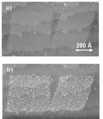
Titanium tetrachloride deposition on the patterned monohydride Si(001)-(2x1) surface at 475K produces highly selective growth of Ti. Figure 1a shows a surface from which the hydrogen resist layer has been removed locally in the shapes of a square and a parallelogram. Figure 1b shows that Ti is selectively adsorbed on the clean Si area after dosing a surface with 6×10⁻² L of TiCl4 , while the resist layer is preserved. Ti atoms form small rows in the initial stages of CVD of Ti.(16) Identification of Ti is made by comparing our images with the STM observations of the physical vapor deposition studies of Ti on Si(001).(23) Remarkably, although we observed Ti and Cl on the clean Si area, neither Cl nor TiCl4 reacted with the hydrogen in the resist layer at substrate temperatures up to 575K. This implies that the Si monohydride surface is not as reactive as the di- or higher hydride phase with which Cl reacts and removes hydrogen as observed by Mendicino.(15)
We observe a Ti growth enhancement in the growth area at the boundary as is seen in Fig 1b. The enhancement comes from excess TiCl4 which diffuses onto the clean Si area from the adjacent monohydride surface. We can estimate the mean free length for TiCl4 on clean Si by comparing the density of Ti atoms near edges of the clean Si with the density of Ti near the center. The mean free path for TiCl4 diffusion before decomposing on clean Si(001) is 10Å. A similar enhancement was previously observed after dosing a patterned Si(001) surface with an Au precursor by Lyding et al.(3) Such an enhancement effect was not observed in our previous experiment on the selective growth of Al using dimethylaluminum hydride (DMAH).(9)

FIG. 1. STM images showing the initial stage of selective Ti deposition on a patterned Si(001) surface at 475K. (a) In the brighter area, the monohydride layer has been removed. (b) After exposure to TiCl4 (0.06L), titanium atoms are selectively deposited on the brighter area. The density of Ti is enhanced at the edges.
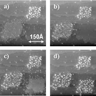
Continued dosing of TiCl4 produces Ti cluster growth. However, the growth is quickly limited by Cl passivation of the reactive dangling and p bonds on the Si surface and presumably the Ti clusters’ surfaces. When there are no available sites for adsorption and reaction of TiCl4, growth stops. For our growth conditions, growth stops after a 1.5L dose of TiCl4. To confirm this, the process of removing H and exposing the surface to TiCl4 was repeated several times. See Fig. 2a, b, c, and d. No further Ti growth is observed for the box in the upper right corner during subsequent doses of TiCl4, while clusters grow on new bare Si areas. The final cluster density in each box is nearly equal, as seen in Fig. 2d.

FIG. 2. A sequence of STM images showing self-limiting growth of Ti clusters on the patterned Si(001) surface at 525K. (a) The upper right box shows the result of an earlier deposition of 2L TiCl4. Another box shaped area of clean Si area is made. (b) The same surface after exposure to 0.1L of TiCl4 on the surface. (c) and (d) Consecutive removing hydrogen and dosing 1.5L TiCl4. The density of Ti is nearly same in the three boxes. There is no accumulation in the box on upper right during the additional TiCl4 exposure processes.
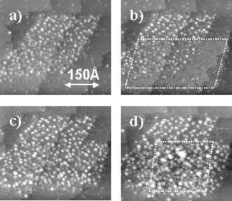
We can restart theTi growth by locally removing the Cl passivation. The Cl was removed by the STM with the same bias voltage and current set as are used to remove the hydrogen.(2) Figure 3b shows an outlined area that has undergone chlorine desorption. In this area, Cl and hydrogen that passivate the dangling bonds or p bonds of the Si(001) surface are removed. There is no evidence of contaminants adsorbing during the process. However, 50% of the Ti clusters have either a reduced height or size. This effect is most likely due to etching of Ti by Cl when the Cl desorbs. After exposing the surface to TiCl4, the density of Ti clusters where Cl was removed is higher than that in the remaining area as is shown in Fig. 3c. Fig. 3d shows that repeating the process of Cl removal followed by TiCl4 exposure ten times allow Ti clusters to approach a thin film. The precision of the STM patterned hydrogen resist can provide feature dimensions as small as 3nm.(2, 9)
We believe that this technique can be used to form nanoscale TiSi2 using the self aligned silicide process by elevating the substrate temperature above 675K. Due to the favorable diffusion into bulk with respect to diffusion on a Si surface, the small feature size should be maintained during the annealing.(24) Alternatively, these nanoscale silicide processes may work for cobalt, platinum, nickel, and palladium by annealing the substrate with the deposition material, if the patterned surface provides selective CVD growth.(25) Platinum and palladium are especially favored since the silicide processes for these materials occur at low enough temperatures for selective CVD with the hydrogen resist.

FIG. 3. A sequence of STM images showing Ti film growth with STM stripping. (a) Initial Ti deposition (0.5L) on a patterned surface. (b) Cl and hydrogen removal by an STM in the box. (c) Exposure of TiCl4 (0.5L). The density of Ti clusters is higher in the overlapped area. (d) Repeating the Cl removal in the box followed by TiCl4 exposure ten times allows Ti clusters to approach a thin film.
We believe that this technique can also be extended to form nanoscale TiN structures. One method would be to use a TiCl4 + NH3 mixture for the CVD growth.(14) However, the limitation of the processing temperature to 625K will result in a 5% of Cl concentration in the film.(14) In practice, this Cl concentration might shorten the lifetime and increase the resistivity of the device. To avoid this problem, the SiO2 resist can be used.(4) The oxide resist allows the CVD processing temperatures up to 950K (27) although the minimum structure sizes is eventually in the range of 300Å to 450Å. (28) Near 950K, the concentration of Cl in the TiN film reduces to 1%.(14) Alternatively, tetrakis dimethyl amino titanium (TDMAT) or tetrakis diethyl amino titanium (TDEAT) with NH3 can provide TiN film growth at a lower deposition temperature of 525K. (29) Using either of these precursors in the selective CVD process with the hydrogen resist would avoid Cl concentration.
In conclusion, We have formed nanoscale Ti structures on the Si(001) surface using the CVD precursor TiCl4 and an atomic hydrogen resist. TiCl4 does not react with the monohydride resist layer. The self limiting of Ti cluster growth by Cl passivation of the surface is observed by STM. Continued Ti growth can be achieved by iterative CVD of Ti using TiCl4 and STM removal of Cl. We have demonstrated that ten iterations of this process allows Ti growth to approach that of a thin film.
References and Notes
(1) C. R. K. Marrian, Ed., Technology of Proximal Probe Lithography (SPIE Institutes, Washington, 1994); C. F. Quate, Surface Science, 386, 259 (1997).
(2)T-C. Shen, C. Wang, G.C. Abeln, J.R. Tucker, J.W. Lyding, Ph. Avouris, and R.E. Walkup, Science 268, 1590 (1995); J.W. Lyding, T. -C. Shen, J.S. Hubacek, J.R. Tucker, and G.C. Abeln, Appl. Phys. Lett. 64, 2010 (1994).
(3)J.W. Lyding, K. Hess, G.C. Abeln, D.S. Thompson, J.S. Moore, M.C. Hersam, E.T. Foley, J. Lee, Z. Chen, S.T. Hwang, H. Choi, Ph. Avouris, and I.C. Kizilyalli, Appl. Surf. Sci. 130, 221 (1998).
(4)M. Shibata, Y. Nitta, K. Fujita, and M. Ichikawa, Appl. Phys. Lett. 73, 2179 (1998).
(5)H. Dai, N. Franklin, and J. Han, Appl. Phys. Lett. 73, 1508 (1998).
(6)T.-C. Shen, C. Wang, and J. R. Tucker, Phys. Rev. Lett. 78, 1271 (1997).
(7)T. Hashizume, S. Sekine, M. I. Lutwyche, S. Watanabe, K. Nakajima, T. Nishi, and Y. Wada, Jpn. J. Appl. Phys 35, L1085 (1996).
(8)D.P. Adams, T. M. Mayer, and B. S. Swartzentruber, Appl. Phys. Lett. 68, 2210 (1996); J. Vac. Sci. Technol. B 14, 1642 (1996).
(9)T. Mitsui, E. Hill, and E. Ganz, J. Appl. Phys. 85, 522 (1999).
(10)G. E. Georgiou, H. Abiko, F.A. Baiocchi, N. T. Ha, and S. Nakahara, J. Electrochem. 141, 1351 (1994).
(11)S. P. Murarka, J. Vac. Sci. Technol. B 4, 1325 (1986); C. M. Osburn, Q. F. Wang, M. Kellam, C. Canovai, P.L. Smith, G. E. McGuire, Z. G. Xiao, and G. A. Rozgonyi, Appl. Surf. Sci. 53, 291 (1991).
(12)S-K. Rha, S-Y. Lee, W-J. Lee, Y-S, Hwang, C-O. Park, D, W, Kim, Y-S Lee, and C-N. Whang , J. Vac. Sci. Technol. B 16, 2019 (1998).
(13)K. Sugai, H. Okabayashi, T. Shinzawa, S. Kishida, A. Kobayashi, T. Yako, and H. Kadokura, J. Vac. Sci. Technol. B 13, 2115 (1995); M.E. Gross, K. P. Cheung, C.G. Fleming, J. Kovalchick, and L. A. heimbrook, J. Vac. Sci. Technol. A 9, 57 (1991).
(14)A. Sherman, J. Electrochem. Soc. 137, 1892 (1990); N. Yokoyama, K. Hinode, and Y. Homma, ibid. 138, 190 (1991); R.W. Fiordalice, R.I. Hegde, and H. Kawasaki, ibid. 143, 2059 (1996); R.I. Hegde. R.W. Fiordalice, E.O. Travis, and P.J. Tobin, J. Vac. Sci. Technol. B 11, 1287 (1993).
(15)M.A. Medicino and E.G. Seebauer, Surf. Sci. 277, 89 (1992); J. Electrochem. Soc. 140, 1786 (1993); R.P. Southwell and E.G. Seebauer, J. Vac. Sci. Technol. A 13, 221 (1995); J. Electrochem. Soc. 144, 2122 (1997).
(16)T. Mitsui, R. Curtis, and E. Ganz, (in progress).
(17)G.C. Abeln, M.C. Hersam, D.S. Thompson, S.-T. Hwang, H. Choi, J.S. Moore, and J.W. Lyding, J. Vac. Sci. Technol. B 16, 3874 (1993).
(18)Silicon (001) samples are 5 × 10 × 0.5 mm3 pieces of p-type, boron-doped wafers with r = 0.1 W cm.
(19)B. S. Swartzentruber, Y. W. Mo, M. B. Webb, and M. G. Lagally, J. Vac. Sci. Technol. A 7, 2901 (1989).
(20)J. J. Boland, Phys. Rev. Lett. 65, 3325 (1990).
(21)TiCl4 (99.9%) is purchased from Aldrich.
(22)We roughly estimate the pressure on the Si surface as double the pressure measured by the ion gauge by comparing the ratio of the number of molecules adsorbed to the number of molecules induced assuming unity sticking probability of TiCl4 (reference 15).
(23)K. Ishiyama and Y. Taga, Phys. Rev. B. 51, 2380 (1995).
(24)B.D. Yu, Y. Miyamoto, O. Sugino, T. Sasaki, and T. Ohno, Phys. Rev. B 58, 3549 (1998).
(25)M.Y. Lee and P.A. Bennett, Phys. Rev. Lett. 75, 4460 (1995).
(26)625K marks the onset of hydrogen resist pattern degradation due to the hydrogen diffusion.
(27)M. Ichikawa, (private communication).
(28)Due to the angular divergence of the field emission beam (70eV-150eV) from the STM tip to selectively remove the SiO2 mask, the smallest dimensions of the silicon structures is in the range of 300Å to 450Å. This feature size limitation might be improved by using nanotips (reference for nanotips, V. Binh, V. Semet, and N. Garcia, Appl. Phys. Lett. 65, 2493 (1994)).
(29)J.A. Prybyla, C-M.Ching, and L.H. Dubois, J. Electrochem. Soc. 140, 2695 (1993); S.C. Sun and M.H. Tsai, Thin Solid Films 253, 440 (1994).
The authors would like to acknowledge Eric Hill and Byron Freelon for suggestions, Jolin Jegier for assistance in handling the TiCl4, and Wayne Gladfelter for helpful discussions and for suggesting this growth system. This work was supported by NSF grant # DMR-9508637.
Jump to
Copyright 1999 by the Regents of the University of Minnesota, Dept. of Physics & Astronomy. All rights reserved.